New factory opened exclusive
for new material wafer processing
2017/01~
~New materials:SiC,Sapphire,LT,etc~
●Increased processing capacity to cope with mass-production.
●Separated from silicon wafer processing, wafer incoming~
delivery to be one-pass process.
●Cost advantage by the process reduction.
●Mass production started in March, 2017.
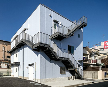
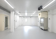
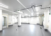
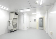
■ New factory image
※New factory(D building) overview
3F Cleaning/Outgoing Inspection
2F Polishing room
1F Grinding
■ Strength
of new factory
High quality achievement of "Flatness", "Surface roughness", "Work-affected layer"
by use of high-rigidity grinder
⇒Reduction of process cost.
Reduction of sleigh after back-grind thinning.
⇒Capable of one-pass processing of grinding + polishing.
High level cleanness by introduction of exclusive
cleaning equipment for Siapphire
(Reduction of contamination + particle)
Expect to introduce knife-edge prevention
process for Sapphire, which is already under operation for
silicon.
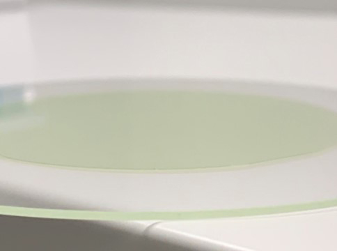
■ Thinning
process of patterned SiC wafer
Example of patterned SiC wafer processing
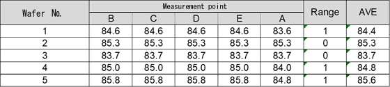
Result of thickness variations of grinded wafer (SiC 6-inch
wafer)
Unit:um
※TV5: 1um≧ after grinding
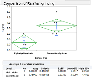
Result of roughness comparison after grinding
(SiC 6-inch wafer)
Thickness variations/surface
roughness improved by use of High rigidity grinder.
※Surface roughness improved with conventional grinder.
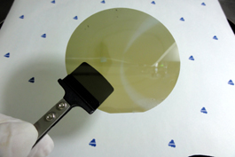
■ Ultra-Thin
SiC wafer processing
Sample data of SiC wafers processed with
wafer support.
4” SiC wafer used to achieve ultra-thin & ultra-flat.
※Result of thickness variations of grinded wafe (SiC 4-inch
wafer)
Backggrinding
4 inch SiC
TV5 (um)
Range
A
B
C
D
E
22.88
22.4
22.03
22.75
22.31
0.37
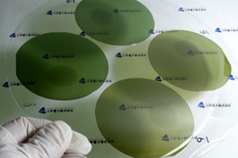
■ SiC wafer grinding and polishing services
Rokko is one of the few companies that provides an integrated SiC
wafer processing service (Wafer grinding, polishing and RCA cleaning)
through its soley develped technologies.
Rokko has developed techniques to utilize its existing semiconductor
tools and equipment for SiC operations. In comparison of the conventional
equipment available in the SiC industry, Rokko’s process has its
advantages in throughput, wafer warpage, roughness, and flexibility
of wafer size.
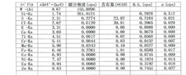
● Total reflection x-ray fluorescence
analysis tool TREX610
Measurable elements: 12 elements (S, Cl, K, Ca, Ti, Cr,Mn,Fe,Co,Ni,Cu,Zn)
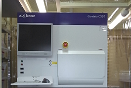
● Candela CS20 Wafer surface
inspection machine
Wafer Size: 3, 4, 5, and 6 Inch
Measurable thickness: 300-1400um
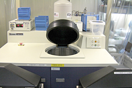
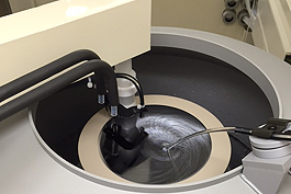
■ Automatic
scrub cleaning process
■ New equipment:
After polishing, residues contain alkaline substances results in
becoming polishing marks or sources of particle. Removing such residues
before coated by native oxide films is one of the key techniques
in polishing.
In our conventional process, wafers are cleaned piece by piece through
operator’s manual scrubbing. Now, Rokko introduced the automated
cleaning equipment to eliminate human errors and deviation of quality
to achieve the uniform stable quality.
■Wafer Size:4, 5, 6, 8 inch
■Thickness:~ 100μm
■Patterned・ MEMS and SOI Wafer
Glass supported wafers also can be processed.
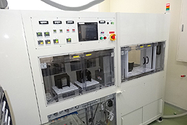
● Automatic scrub cleaning machine
High cleaning performance.
● Automatic scrub cleaning machine
Wafer Size: 4, 5, 6, 8 Inch
Sapphire and SiC wafers can be processed
■ SiC
wafer process
Comparison of SiC wafer process
Conventional process
Rokko's process
Diamond lapping
Polishing, CMP
Grinding
Polishing, CMP
Running cost
High
(Metal wheels + Diamonds)
Moderate
(Pads + Slurry)
Moderate
(Diamond wheels)
Moderate
(Pads + slurry)
Required level of process technology
High
Moderate
High
High
Cost of equipment
High
Moderate
High
High
Throughput
Very low
Low
Moderate
Moderate
Remarks
Wax mounting
Difficulties in lapping table adjustment
Higher number of process is required.
Wax mounting
Difficulties in lapping table adjustment
Vacuum chucking system.
Automatic grinding machine for sapphire and .SiC
Waxless polishing
■ SiC
wafer grinding process-Roughness
150mm SiC wafer grinding surface
roughness
Evaluation
Rough grinding
Final grinding
Roughness
Ra
12.4-14.6nm
2-5nm
Warp
Visual(Scale)
0.5-0.8mm
0.2-0.4mm
※Surface roughness:Non-contact type surface
profile measuring equipment :Zygo
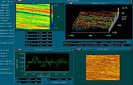
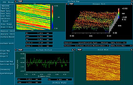
■ SiC
wafer CMP surface AFM measuring result
(6 inch)
6 inch SiC surface polishing
surface AFM measurement result
(3 points of surface)
Center
Ra:0.711Å
Middle
Ra:0.576Å
Edge
Ra:0.632Å
150mm SiC wafer
Si surface post CMP surface roughness Ra < 0.1nm
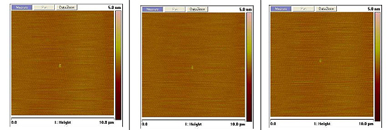
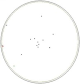
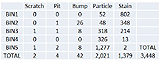
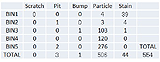
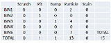
■
SiC wafer post cleaning particle measurement result
150mm SiC
wafer post cleaning particle measurement result
Pre cleaning
Scrub cleaning
RCA cleaning
1.Scrub cleaning is effective for emoving large
size particle
2Particles and dirt are removed after RCA cleaning
3.10 pieces≧0.3um
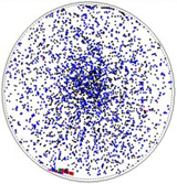
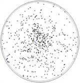
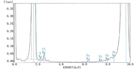
■ Metal
contamination after SiC wafer cleaning
150mm SiC
wafer metal contamination after wafer cleaning
TXRF tester
Result of measuring(by TRFX) SiC wafer
cleaning process