We also offer paid contract testing services
for inspections only. Please feel free to contact us.
■ Inspection correspondence
table by material
○-Mark = Inspection available Each material * Each inspection
details
Material
Face
Particles
Contamination
Flatness
Thickness
ICP-MS
TXRF
Zygo
TTV
SBIR
SFQR
BOW
Warp
SORI
contact type
non-contact type
Resistance
P/N
MEM
SICA
Silicon
○
○
○
○
○
○
○
○
○
○
○
○
○
○
○
N-dope SiC
Si-face
○
○
○
○
○
○
○
○
○
○
○
○
○
C-face
○
○
○
○
○
○
○
○
○
○
○
○
○
Semi-insulating
SiC
Si-face
○
○
○
○
○
○
○
○
○
○
○
○
C-face
○
○
○
○
○
○
○
○
○
○
○
○
SiC Epi wafer
○
○
○
○
○
○
○
○
○
○
○
○
○
Polycrystalline SiC
○
○
○
○
○
○
○
○
○
○
○
○
LiTaO 3
○
○
○
○
○
○
○
○
○
○
○
LiNbO3
○
○
○
○
○
○
○
○
○
○
○
GaN
Ga-face
○
○
○
○
○
○
○
○
○
○
○
N-face
○
○
○
○
○
○
○
○
○
○
○
Sapphire
C-face
○
○
○
○
○
○
○
○
○
○
○
R-face
○
○
○
○
○
○
○
○
○
○
○
Ga2O3
○
○
○
○
○
○
○
○
○
○
○
AlN
Al-face
○
○
○
○
○
○
○
○
○
○
○
N-face
○
○
○
○
○
○
○
○
○
○
○
Quartz
○
○
○
○
○
○
○
○
○
○
○
○
GaN on Si
○
○
○
○
○
○
○
○
○
○
○
○
GaN on Sap
○
○
○
○
○
○
○
○
○
○
○
○
GaN on SiC
○
○
○
○
○
○
○
○
○
○
○
○
SOI
○
○
○
○
○
○
○
○
○
○
○
○
○
Oxide film
○
○
○
○
○
○
○
○
○
○
○
○
○
○
Glass
○
○
○
○
○
○
○
○
○
○
○
○
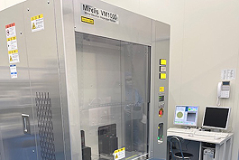
● Mirelis electron microscope 【MEM】
※8-inch SiC measurement available
※Contract inspection services available.
Used as a surface (Si surface) latent flaw inspection machine
to check for processing damage and defects.
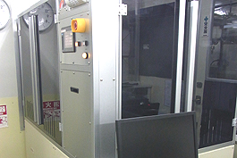
● SiC wafer defect inspection and review system 【SICA88】
※8-inch SiC measurement available
※Contract inspection services available.
Used for scratch inspection of surfaces (Si side and C side),
and for checking pits, defects, etc.
● Wafer flatness measurement
and analysis system
【Tropel】
※Contract inspection services available.
Used to check flatness before and after processing.
TTV, NTV, SORI, BOW, WARP, etc.
● Surface roughness measuring
instrument 【Zygo】
※Contract inspection services available.
Used for checking surface roughness after machining (non-contact
measurement).
Roughness measurement after grinding and CMP (Chemical Modulation).
● Total Internal Reflection X-ray
Fluorescence Analyzer 【TXRF】
※Contract inspection services available.
Metal contamination and full-surface sweep measurement possible《[S
Cl K Ca Ti Cr Mn Fe Co Ni Cu Zn》
● Inductively coupled plasma
mass spectrometer
【ICP-MS】
※Contract inspection services available.
Metal contamination and various metals can be measured
● Particle counter
We inspect the particles in the polished wafer.
● Flatness measuring device
We will measure the BOW, WARP, and TTV of the polished wafer.
● Automatic spectral interference
wafer thickness meter
Thickness can be measured for the silicon layer only of the
taped wafer・SOI・supported wafer・resin-material/tape supported
wafer(in case 2 silicon wafers are attached, one side silicon
layer can be measured).
This equipment unloads wafers from cassettes and measures
thickness at a designated coordinate of wafer. The measurement
is done by a contactless capacitance sensor.
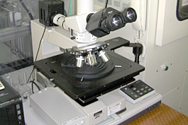
Differential interference contrast
microscope
This tool allows to observe roughness on a wafer surface.
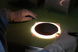
Visual inspection
Wafers are inspected under a halogen lamp in a dark room.